Lead Sulfide IR Multiplexed Linear Arrays
Array
- PbS Array 1-3 microns
- PbS Array 1-3 microns
- PbSe Array 1-5 microns
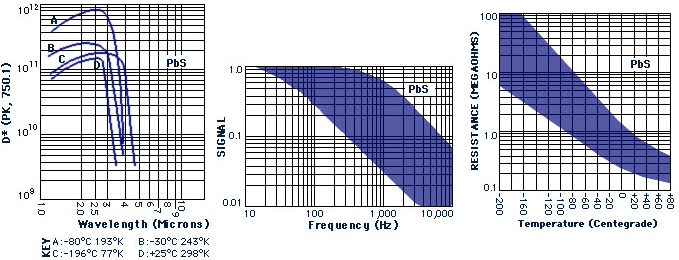
- PbS D* >8 x 10¹⁰ Note
- PbSe D* >3 x 10⁹ Note
- Square or rectangular geometry
- Pitch down to 59 microns
- Pixels 256
- Thermoelectrically cooled
- TE Cooler Controller
- Operating temp. down to 253K
- Optical filters
- Low cost
- Custom designs
Multiplexing
- DC integrating
- Dark current subtraction
- Sample rates from 100 Hz to 1.2 MHz
- Independent or slave operation
- Custom interfaces available
- Integration times from 0.05 msec to 0.66 sec.
System Requirements
- ±12 to ±15VDC
- TE Cooler 5V @ 2 amps (typical)
Amplifier Specifications
- Output voltage range up to ±12V
- Output current 2-3 mAmp typical and up to 30 mAmp available
- Adjustable output gain available>
Signal Processing
New England Photoconductor Corp. has demonstrated a unique approach to multiplexing PbS and PbSe arrays which fully integrates the signal from every detector. This innovative concept provides a method for monitoring the signals from a large number of photoresistive detectors. The result is minimal degradation in signal to noise ratio due to multiplexor timing requirements.
This multiplexing approach accumulates the current from each detector within the array >99% of the time, essentially removing the time dependent degradation of the serial approach. The key to this new method is multiplexing current instead of voltage. Each detector within the array has an associated integration capacitor which accumulates charge at a rate dependent upon the resistance of its pixel.
While this is occurring, the multiplexor circuitry sequentially accesses each integrating capacitor, transferring its charge to an output current to voltage converter. This process discharges the capacitor, allowing the capacitor to recharge for a full array scan period before being accessed again.
The multiplexing system also allows the output leads from the multiplexor to be held at a constant voltage, removing the effects of parasitic capacitance and substantially reducing unwanted EMI effects. In essence, this approach provides a single serial output signal from the array, with similar signal to noise performance as achieved by operating a single detector.
The fully integrating multiplexing technique has clock speeds which can be varied from 100 Hertz to 1.2 MHz. This corresponds to an array scan time (i.e. a detector integration time) of 0.05 milliseconds to 0.66 seconds (for a 64 element array). The current system design is completely self-contained, requiring only the application of ±12 volts ±15 volts and 5 volts @ 2 amps to operate the cooler. The system outputs include a serial analog signal with voltages corresponding to the detector signals, a clock which indicates when data is good, and a start of array scan pulse to register the data to the beginning of the array.
Many variations to this system can be provided to allow custom interfacing of the fully integrating multiplexor system to an end user’s application. Features such as adjustable clock speed, a user supplied clock (i.e. slave operation), active modulation of the bias voltage to allow AC illumination operation, and additional output signal processing are all available. Please email EOC for further information on applying this exciting new multiplexing approach to your application.
PbS Response Chart